- 您现在的位置:买卖IC网 > Sheet目录477 > MICRF501BLQ TR (Micrel Inc)TXRX SGL 300-600MHZ 44-LQFP
�� �
�
�MICRF501�
�Applications� Information�
�VCO� and� PLL� Section�
�DIFV� DD�
�Micrel�
�The� frequency� synthesizer� consists� of� a� VCO,� crystal� oscilla-�
�tor,� dual-modulus� prescaler,� programmable� frequency� divid-�
�C36�
�1n�
�Pin� 12�
�ers,� phase-detector,� charge� pump,� lock� detector� and� an�
�external� loop� filter.� The� dual-modulus� prescaler� divides� the�
�VCO-frequency� by� 32/33.� This� mode� is� controlled� by� the� A-�
�10MHz�
�C20�
�2-6p�
�C22�
�5.6p�
�Pin� 13�
�XOSCOUT�
�divider.� There� are� two� sets� of� M,� N� and� A-frequency� dividers.�
�Using� both� sets� in� transmit� mode,� FSK� can� be� implemented�
�by� switching� between� those� two� sets.� The� phase-detector� is�
�a� frequency/phase� detector� with� back� slash� pulses� to� mini-�
�mize� phase� noise.� The� VCO,� crystal� oscillator,� charge� pump,�
�lock� detector� and� the� loop� filter� will� be� described� in� detail�
�below.�
�Voltage� Controlled� Oscillator� (VCO)�
�C21�
�47p�
�DIGGND�
�Figure� 4.� Crystal� Oscillator�
�The� crystal� oscillator� is� tuned� by� varying� the� trimming� capaci-�
�tor� C20.� The� drift� of� the� RF� frequency� is� the� same� as� the� drift�
�of� crystal� frequency� when� measured� in� ppm.� The� total� differ-�
�ence� in� ppm,� ?� f(ppm),� between� the� tuned� RF� frequency� and�
�C13�
�VDD�
�Pin� 5�
�R7�
�3.6k�
�the� drifted� frequency� is� given� by:�
�?� f(ppm)� =� S� T� � ?� T� +� n� � ?� t�
�where:�
�loopfilter_output�
�R8�
�47k�
�D1�
�MA4ST350�
�L1�
�47nH�
�C35�
�2.2p�
�15p�
�Pin� 6�
�OSCOUT�
�?�
�?�
�S� T� is� the� total� temperature� coefficient� of� the� oscillator�
�frequency� (due� to� crystal� and� components)� in� ppm� °� C.�
�?� T� is� the� change� in� temperature� from� room�
�temperature,� at� which� the� crystal� was� tuned.�
�Pin� 7�
�?�
�n� is� the� ageing� in� ppm/year.�
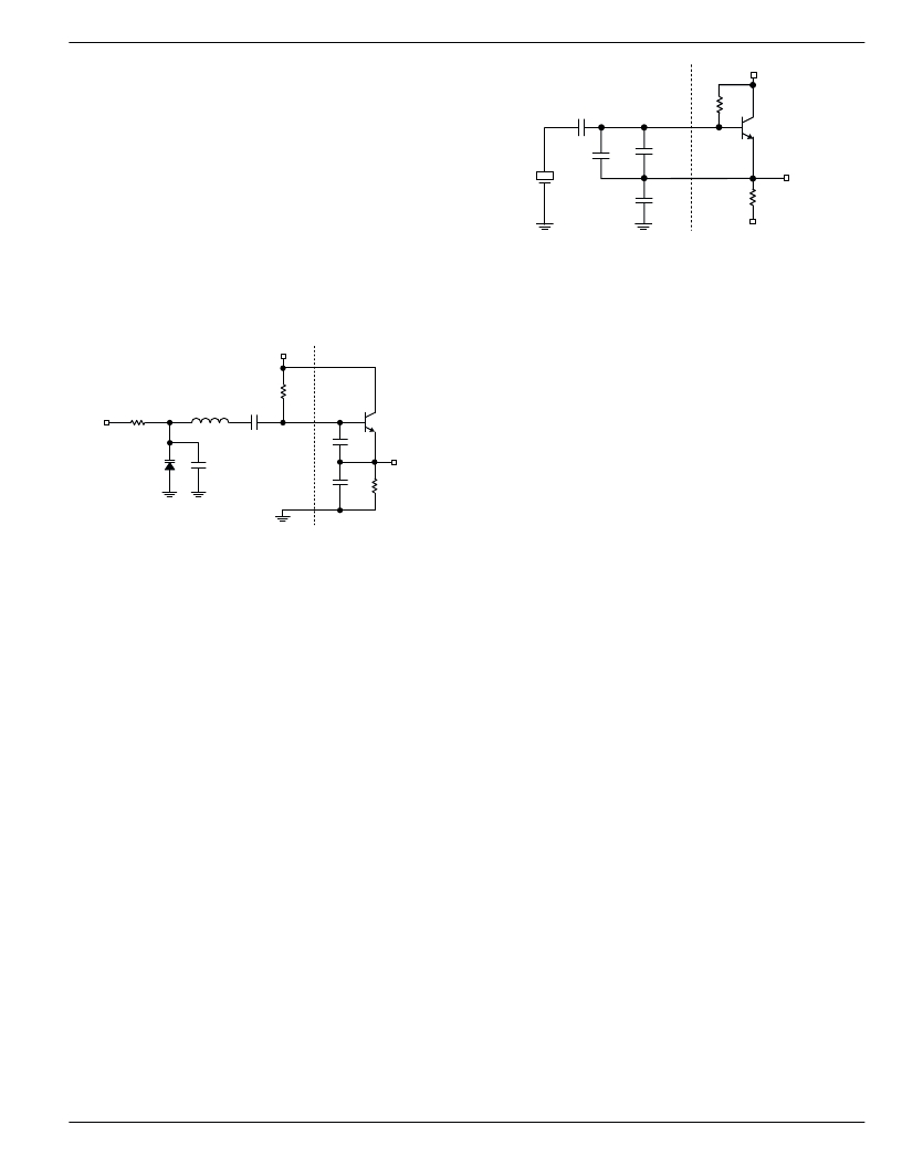
�Figure� 3.� VCO�
�?�
�?� t� is� the� time� (in� years)� elapsed� since� the� transceiver�
�was� last� tuned.�
�The� circuit� schematic� of� the� VCO� with� external� components�
�is� shown� in� Figure� 3.� The� VCO� is� basically� a� Colpitts� oscilla-�
�tor.� The� oscillator� has� an� external� resonator� and� varactor.�
�The� resonator� consists� of� inductor� L1� and� the� series� connec-�
�tion� of� capacitor� C13,� the� internal� capacitance,� the� capaci-�
�tance� of� the� varactor� and� C35� in� parallel� with� D1.� The�
�capacitance� of� the� varactor� (D1)� decreases� as� the� input�
�voltage� increases.� The� VCO� frequency� will� therefore� in-�
�crease� as� the� input� voltage� increases.� The� VCO� has� a�
�positive� gain� (MHz/Volt).� C35� is� added,� if� necessary,� to� bring�
�VCO� tuning� voltage� to� its� middle� range� or� VCC/2,� which� is�
�measured� at� Pin� 9� -� CMPOUT.�
�If� the� value� of� capacitor� C13� and� C14� become� too� small� the�
�amplitude� of� the� VCO� signal� decreases,� which� leads� to� lower�
�output� power.�
�The� layout� of� the� VCO� is� very� critical.� The� external� compo-�
�nents� should� be� placed� as� close� to� the� input� pin� (Pin� 6)� as�
�possible.� The� anode� of� the� varactor� D1� must� be� placed� next�
�to� pins� 7� and� 8.� Ground� vias� should� be� next� to� component�
�pads.�
�Crystal� Oscillator�
�The� crystal� oscillator� is� the� reference� for� the� RF� output�
�frequency� as� well� as� for� the� LO� frequency� in� the� receiver.� The�
�crystal� oscillator� is� a� very� critical� block� since� very� good� phase�
�and� frequency� stability� is� required.� The� schematic� of� the�
�crystal oscillator with external components for 10MHz is�
�shown� in� Figure� 4.� These� components� are� optimized� for� a�
�crystal� with� 15pF� load� capacitance.�
�The� demodulator� will� not� be� able� to� decode� data� when�
�?� f(Hz)� =� ?� f(ppm)� � f� RF� is� larger� than� the� FSK� frequency�
�deviation.� For� small� frequency� deviations,� the� crystal� should�
�be� pre-aged,� and� should� have� a� small� temperature� coeffi-�
�cient.� The� circuit� has� been� tested� with� a� 10MHz� crystal,� but�
�other� crystal� frequencies� can� be� used� as� well.�
�The� circuit� has� been� tested� with� a� 10MHz� crystal,� but� other�
�crystal� frequencies� can� be� used� as� well.�
�Prestart� of� XCO�
�The� start-up� time� of� a� crystal� oscillator� is� typically� some�
�milliseconds.� Therefore,� to� save� current� consumption,� the�
�MICRF501� circuit� has� been� designed� so� that� the� XCO� is�
�turned� on� before� any� other� circuit� block.� During� start-up� the�
�XCO� amplitude� will� eventually� reach� a� sufficient� level� to�
�trigger� the� M-counter.� After� counting� two� M-counter� output�
�pulses� the� rest� of� the� circuit� will� be� turned� on.� The� current�
�consumption� during� the� prestart� period� is� approximately�
�300� μ� A.�
�Lock� Detector�
�The� MICRF501� circuit� has� a� lock� detector� feature� that� indi-�
�cates� whether� the� PLL� is� in� lock� or� not.� A� logic� high� on� Pin� 15�
�(LOCKDET)� means� that� the� PLL� is� in� lock.�
�The� phase� detector� output� is� converted� into� a� voltage� that� is�
�filtered� by� the� external� capacitor� C23,� connected� to� Pin� 14,�
�LDC.� The� resulting� DC� voltage� is� compared� to� a� reference�
�window� set� by� bits� Ref0� –� Ref5.� The� reference� window� can� be�
�stepped� up/down� linearly� between� 0V,� Ref0� –� Ref5� =1,� and�
�Ref0� –� Ref5� =� 0,� which� gives� the� highest� value� (DC� voltage)�
�of� the� reference� window.� The� size� of� the� window� can� either� be�
�March� 2003�
�9�
�MICRF501�
�发布紧急采购,3分钟左右您将得到回复。
相关PDF资料
MICRF505DEV1
KIT DEV RADIOWIRE 850-950MHZ
MICRF506DEV1
EVAL BOARD EXPERIMENTAL MICRF506
MICRF507YML TR
TXRX FSK LOW PWR W/AMP 32MLF
MICRF600DEV1
KIT DEV RADIOWIRE 902-928MHZ
MK01-C
SENSOR REED SPST-NO SMD
MK01-H
SENSOR REED SPDT-CHANGE SMD
MK02/0-1A66-500W
SENSOR REED SPST-NO
MK02/6-0
SENSOR REED PCB 24MM T/H
相关代理商/技术参数
MICRF501EVAL1
功能描述:EVAL BOARD EXPERIMENTAL MICRF501 RoHS:否 类别:RF/IF 和 RFID >> RF 评估和开发套件,板 系列:RadioWire® 标准包装:1 系列:- 类型:GPS 接收器 频率:1575MHz 适用于相关产品:- 已供物品:模块 其它名称:SER3796
MICRF505
制造商:MICREL 制造商全称:Micrel Semiconductor 功能描述:868MHz and 915MHz ISM Band Transceiver
MICRF505_07
制造商:MICREL 制造商全称:Micrel Semiconductor 功能描述:850MHz and 950MHz ISM Band Transceiver
MICRF505BML
制造商:Rochester Electronics LLC 功能描述: 制造商:RF Micro Devices Inc 功能描述:
MICRF505BML TR
功能描述:TXRX ISM 868-915MHZ 32-MLF RoHS:否 类别:RF/IF 和 RFID >> RF 收发器 系列:- 产品培训模块:Lead (SnPb) Finish for COTS
Obsolescence Mitigation Program 标准包装:30 系列:- 频率:4.9GHz ~ 5.9GHz 数据传输率 - 最大:54Mbps 调制或协议:* 应用:* 功率 - 输出:-3dBm 灵敏度:- 电源电压:2.7 V ~ 3.6 V 电流 - 接收:* 电流 - 传输:* 数据接口:PCB,表面贴装 存储容量:- 天线连接器:PCB,表面贴装 工作温度:-25°C ~ 85°C 封装/外壳:68-TQFN 裸露焊盘 包装:管件
MICRF505DEV1
功能描述:射频开发工具 MICRF505 Evaluation Kit - For experimental use only
RoHS:否 制造商:Taiyo Yuden 产品:Wireless Modules 类型:Wireless Audio 工具用于评估:WYSAAVDX7 频率: 工作电源电压:3.4 V to 5.5 V
MICRF505DEV1
制造商:Micrel Inc 功能描述:KIT MICRF505 EVALUATION
MICRF505L
制造商:MICREL 制造商全称:Micrel Semiconductor 功能描述:850MHz and 950MHz ISM Band Transceiver